
Instrument Expert
Original factory packaging

Service Hotline:
(+86)010-52867771
Instrument Expert
Original factory packaging
Service Hotline:
(+86)010-52867771
Frank Pan, Senior Application Engineer, CPG Division
Abstract: Switching power supply and Class D power amplifier, because the circuit works in the switching state, greatly reduce the power loss of the circuit, in today's electronic products have been widely used. Because of the existence of parasitic inductance and parasitic capacitance, the PWM switch waveform of the circuit is often accompanied by ringing when it jumps. These rings often cause annoying EMC problems. This paper discusses ringing and uses snubber circuit to suppress ringing on PWM switch signal.
In switching power supply and Class D power amplifier circuits, ringing is mostly caused by the parasitic inductance and parasitic capacitance of the circuit. Parasitic inductance and parasitic capacitance constitute LC resonant circuit. Two parameters are often used to describe the resonant characteristics of LC resonant circuits: oscillation frequency( ),Quality factor (Q value). The resonant frequency is determined by the inductance and capacitance:
 。The quality factor can be defined as the ratio of energy stored in a resonant circuit to energy consumed in a cycle. The Q value of the parallel resonant circuit is:
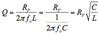 ,Where RP is the equivalent parallel resistance of the parallel resonant circuit. Q value of the series resonance circuit is:
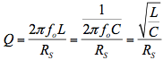 ,RS is the equivalent series resistance of the series resonant circuit.Damping coefficient is commonly used to describe the step jump of LC circuits(
 ) To describe the circuit characteristics. The relation between damping coefficient and quality factor is:
 或
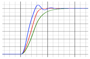
或 .At critical damping(=1),The step signal can jump to the final value in the shortest time, without ringing. Under damping(<1),The step signal is accompanied by a ring when it changes. In over damping(>1),The step signal is not accompanied by ringing when it jumps, but it takes a long time to stabilize to the final value. In Figure 1, the blue, red and green curves are respectively underdamped(<1),Critical damping(=1),Over damping(>1)Corresponding step waveform.
We can easily obtain the damping coefficient of parallel LC resonant circuit: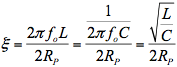 。When we do not change the parasitic inductance and parasitic capacitance of the circuit, the damping coefficient of the resonant circuit can be changed by adjusting the equivalent parallel resistance, thus controlling the ringing of the circuit.
The overshoot of step signal caused by ringing is related to damping coefficient: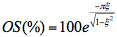 .OS(%)Defined as the ratio of the amplitude of the overimpulse to the amplitude of the signal, expressed as a percentage. Table 1 lists the overshoots corresponding to different damping coefficientsOS(%).
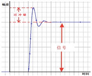
Table 1: Overshoot OS(%) corresponding to different damping coefficients
|
Coefficient of damping |
0.05 | 0.1 | 0.15 | 0.2 | 0.25 | 0.3 | 0.35 | 0.4 | 0.45 |
|
Over impulse |
85.4% | 72.9% | 62.1% | 52.7% | 44.4% | 37.25% | 30.93% | 25.4% | 20.6% |
|
Coefficient of damping |
0.5 | 0.55 |
0.6 |
0.65 | 0.7 | 0.75 | 0.8 | 0.85 | 0.9 |
|
Over impulse |
16.3% | 12.6% | 9.5% | 6.8% | 4.6% | 2.8% | 1.5% | 0.6% | 0.15% |
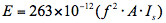 ,The unit is volts per meter. Where f Is the frequency of the current (MHz), A is the loop area of the current (CM2), and is is the current amplitude (mA).
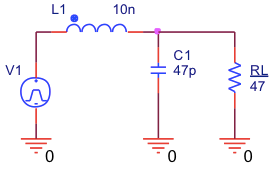
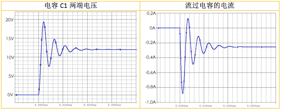
For ringing, we intuitively feel the voltage fluctuation on the oscilloscope screen. It is usually the resonance of the circuit's current that causes the problem. In the circuit shown in FIG. 3, when PWM switch signal V1 switches between 0V and 12V, the resonant current flowing through inductor L1 and capacitor C1 can reach the magnitude of amperes, as shown in FIG. 4. At high frequency (the resonant frequency of the circuit shown in Figure 3 is 232MHz, and the common ringing frequency of switching power supply and Class D circuit is between tens and hundreds of megaHz), ampere-magnitude current passing through a small loop may cause radiation exceeding the standard and make the product fail to pass EMC certification.
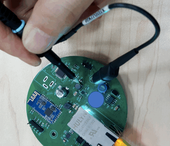
In order to improve the efficiency of the circuit, the PWM switching signal of the switching power supply and Class D power amplifier is relatively short, often in the order of 10ns. To measure such a fast switching signal, it is necessary to consider the influence of oscilloscope probe, especially the probe grounding wire on the measurement results. In the measurement method shown in Figure 5, the ground wire of the oscilloscope probe is too long, forming a large loop with the probe at the tip of the probe. The captured signal has a loud ringing, as shown in Figure 6.
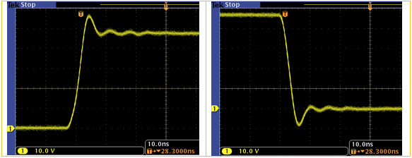
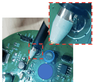
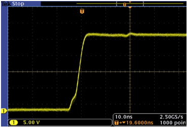
In order to reduce the impact of the oscilloscope probe on the measurement results, we welded the measuring ground probe on the circuit board and removed the ground wire on the oscilloscope probe, as shown in Figure 7. In this way, we can greatly reduce the introduction of the oscilloscope probe ground wire to the measurement of ringing. Figure 8 shows the front and back edge waveforms of the PWM switch signal captured using this method.
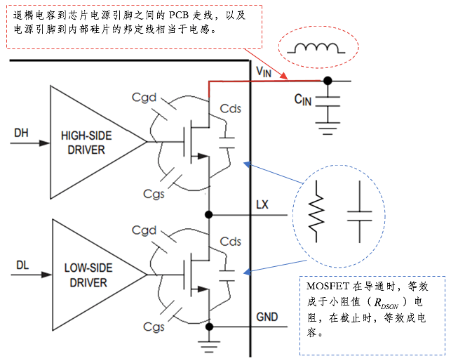
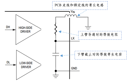
In switching power supply and Class D power amplifier circuits, the PCB line between the chip decoupling capacitor and the chip power pin, and the bond line between the chip power pin and the internal silicon chip can be equivalent to a parasitic inductor. At the cut-off of a power MOSFET, the capacitance (Cgs, Cgd, Cds) between the power MOSFET electrodes can be equivalent to a parasitic capacitance. Figure 9 shows this. These parasitic inductors and capacitors constitute LC resonant circuits. When the high-end MOSFET in FIG. 9 is on and the low-end MOSFET is off, it can be equivalent to the LC resonant circuit shown in FIG. 10. In order to improve the efficiency of the circuit, the integrated power MOSFETs of today's chips are made relatively small, often in the range of tens to hundreds of millieurs. This means that the damping coefficient of a resonant circuit may be very small. The result is a relatively large ring when the PWM switch is switched.
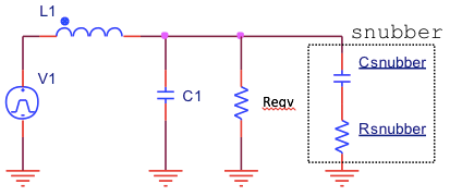
The ringing of LC resonant circuit is described above. The following describes the use of snubber circuit to suppress ringing. As shown by the circuit in the dotted box in Figure 11, the Snubber circuit consists of a small resistance And a capacitor
 A series formation. Resistance in medium用To adjust the damping coefficient of LC resonant circuit. capacitanceAt the ringing frequency (LC resonant frequency), there is a very low tolerance, which is approximately short circuit. The PWM switching frequency also presents a high tolerance. If you don't have a capacitorThe presence of PWM signals will always be added to the resistorBoth ends, resistanceYou use too much energy.
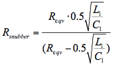
The following isSelect the appropriate resistance value so that the PWM switch signal can be quickly stabilized to the final value without ringing (critical damping). Let's take the circuit in Figure 11 as an example. L1 is the parasitic inductance of the circuit, C1 is the parasitic capacitance of the circuit, and is the equivalent parallel resistance of the circuit.
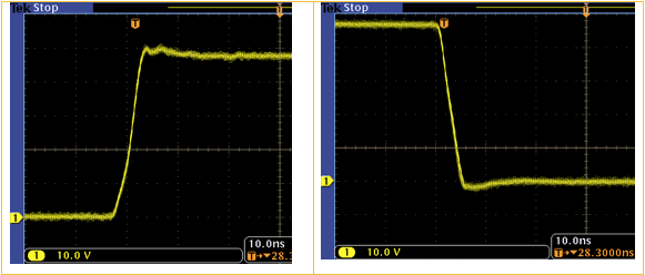
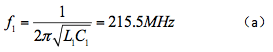
The following is an example of snubber circuit element value selection. Figure 12A is a step-down DC-DC waveform measured at the pin of PWM switch. When the PWM signal is switched on and off, it is accompanied by ringing. The ringing frequency measured by oscilloscope was 215.5MHz. We can construct the first equation:
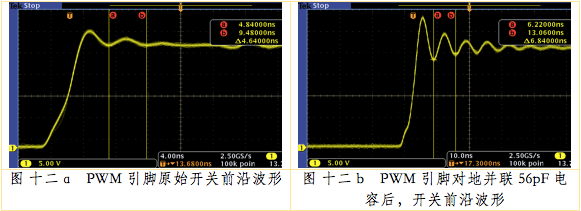
To get the values of L1 and C1, we need to construct another equation. We connect capacitor C1 with a small capacitor in parallel: weld a 56pF capacitor temporarily to the ground on the PWM pin. At this time, the ringing frequency becomes 146.2MHz, as shown in FIG. 12B. From this, we construct another equation:
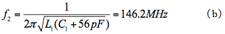
From the above two equations, we can quickly calculate that C1=47.7pF and L1=11.4nH.
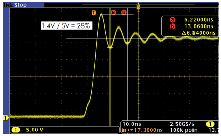
Then, we calculate the equivalent parallel resistance based on the overimpulse . Figure 13 shows that the overshot OS (%) is 28% and the corresponding damping coefficient()The value is 0.37.
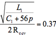 ,get
,get
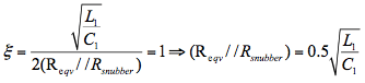
We've got L1, C1 and the circuit the value of phi, which is substituted into the formula we got earlier
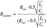 ,Get by calculation
 . You can pick a resistance of 18 ohms.
capacitanceTo choose from:The principle of element value selection is that at LC resonant frequency (ringing frequency), the capacitive reactance is much less thanthe resistance value of For PWM switch signal, but also to present a high enough tolerance.Figure 14 isUsing 560pF capacitance,When 18 ohm resistance is used, the leading edge waveform of PWM switch signal. By contrast with the waveform in FIG. 12A, the ringing has been greatly improved.
In Snubber circuits, energy is consumed in resistance,The amount of energy consumed depends on the capacitancethe capacity, and the resistanceis indpendent of the value of This is because PWM signals give capacitanceWhen charging, the energy provided by the circuit to the snubber circuit is ,Capacitors get only half of that(
 ),The other half waswear. changethe resistance value of the capacitor simply changes the charging speed andenergy is consumed at a rate that does not change once chargedtotal energy consumed.time of discharge,The energy stored by a capacitor isconsumption.The energy consumption in a PWM switching cycle is。The power consumption is:
 ,Among them
 Is PWM switching frequency, V is the peak value of voltage amplitude at both ends of snubber.
Some applications have high requirements on the efficiency of the circuit, and the power consumption of snubber circuit also needs to be limited. In this case, the snubber circuit component values can be adjusted appropriately to strike a balance between the ringing and power consumption of PWM signals.
Another effective way to reduce snubber power consumption is to reduce the parasitic inductance of the circuit: place the decoupling capacitor as close to the chip as possible, and thicken the width of the PCB line between the decoupling capacitor and the chip. From the formula mentioned earlier( )It can be seen that the parasitic inductance L1 is reduced, and a smaller resistance value is needed to maintain the same damping coefficient when other circuit parameters do not change. At the same time, when the parasitic inductance is reduced, the ringing frequency of the circuit will be increased. This all allows us to choose a smaller volumeCapacitance, thus reducing the power loss introduced by snubber circuits.
We discuss the ringing phenomenon of PWM signal in switching power supply and Class D power amplifier circuit, the harm caused by ringing, ringing caused overshoot and the corresponding relationship between the damping coefficient of the circuit. Then it describes how to use snubber to suppress ringing. Finally, an example is given to describe the selection of element value in snubber circuit. In the course of introduction, some simple mathematical formulas are introduced. These mathematical formulas help to deepen our understanding of the concept.
Customer Service QQ
Customer Hotline:
Technical Supports

 3003988120
 yiqi.com
 bio-equip.com
 b2bwork.baidu.com
 baidu.com